by Dan Peirce
Translated from dokuwiki July 20, 2013
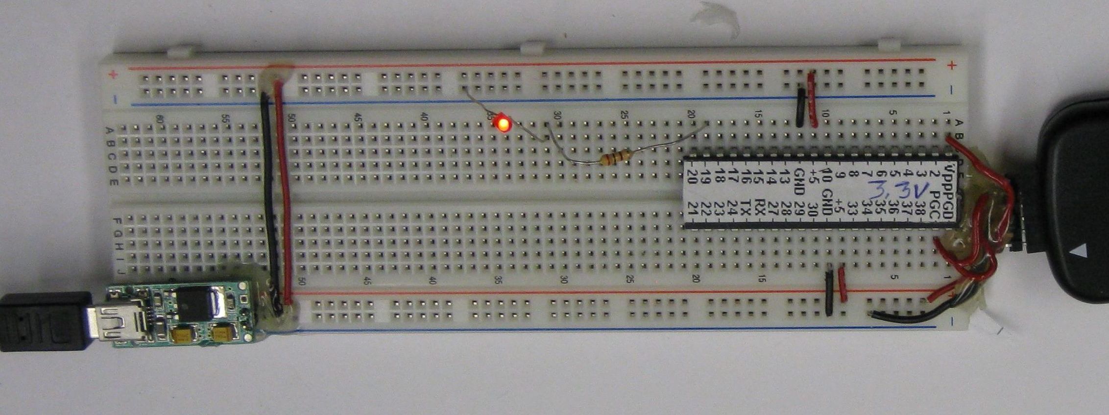
The USB regulator board purchased from Mouser comes preassembled except for the voltage supply pins. The board comes with a three pin breakaway header. I broke off one pin so that the other two could be inserted into the 3.3 volt and ground holes on the regulator board (the unregulated 5V pad/hole left empty). This way the two pins of the header then fit into the power rails of the breadboard. I added jumpers to the solderless breadboard to join the two positive power rails together and to joint the two negative rails together. I also inserted jumpers to the power pins of the PIC IC.
Five wires were used on the programming header. In APSC1299 we only use four wires but I felt it would be better if the students could read the voltage supplied to the PIC in MPlab. The extra wire is for Vdd which lets the PIC read this voltage. Power should be applied to the regulated board before connecting the PICkit2 (otherwise the PICkit2 will not detect the 3.3 volts from the regulator and may attempt to supply 5 volts to the board).
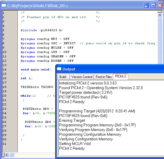
For testing I used the blinkD0.c file from lab3 of APSC1299. The only change required was to explicidly turn off the Brown Out Reset Enable. In the image below both the MPlab IDE output window and some of the BLINK_D0.c code can be seen.
Notice
The #pragma config BOREN = OFF directive
The third line of the output window Target power detected (3.24V).
The PICkit2 detects the PIC18LF4515 as a PIC18F4525 since the only difference is the supply voltage the chip can be used at.
As with the original program the PIC is left at the default internal clock frequency. At 3.3V this MCU should not be clocked at more than 16 MHz.
I have also purchased some PIC18LF2620 MCUs. I believe we do not actually require all the pins available on the PIC18LF4525. The PIC18LF2620 is the same in most respects but it only has 28 pins rather than 40 and comes in a package that is half as wide.
| PIC18LF4525 | PIC18LF2620 |
|---|---|
| Has D port | No D Port |
| Program Memory 48KBytes | Program Memory 64KBytes |
| 1 CCP, 1 ECCP | 2 CCP |
| ADC 13 ch | ADC 10 ch |
| two Vdd pins | only one Vdd pin |
| 40 pins | 28 pins |
| 0.6 inch wide DIP | 0.3 inch wide PIC |
For testing I used the blinkD0.c file from the PIC18LF4525 project.
Changed the file name to blinkB0.c
Changed all references to the D port to the B port.
included p18f2620 rather than p18f4525
Changes to wiring
Popped the PIC18LF4525 out of the breadboard and popped the PIC18LF2620 in.
Moved a ground wire from pin 12 to pin 8 (on the other side of the chip the power and ground did not need to be moved even though the designation of the pins are different they are the same distance from the top of the IC).
Removed a Vdd wire (only one used on the PIC18LF2620)
Moved the LED over to B0 (pin 21).
The Progamming adaptor wiring is the same as the PIC18LF4525.